

| 高级护理(一对一服务) | 普通护理(一或一对多服务 ) | |||||||
| 护理收费标准 | 全护理24 | 全护理24 | ||||||
| 护理服务范围 | 适用于生活完全不能自理的患者: | 适用于部分生活不能自理及轻微病人的患者: | ||||||
|
|
|||||||
IGBT模块封装底板的氧化程度对焊接空洞率的影响分析
黄小娟,王豹子,叶娜,谢龙飞,高凡,刘超
(中国中车永济新时速电机电器有限责任公司——半导体分公司,陕西,西安,邮编:710000)
摘要:本文简介了IGBT模块的主要封装工艺流程,并在相同的实验条件下,对两组不同氧化程度的模块分别进行超声波无损检测扫描,将扫描图像载入空洞统计分析软件,通过对比两组空洞率数据发现:非氧化底板焊接空洞率较低,氧化底板的焊接空洞率普遍偏大。基于本实验的结果,本文建议IGBT模块在封装之前,应对散热底板做好防腐处理,以确保底板不被氧化。
关键词:IGBT;底板;氧化;空洞率;超声波检测
中图分类号:TN305.94 文献标识码:T
Analysis of solder void ratio affected by oxidation degree of the IGBT module packaging base plate
HUANG Xiao-juan, WANG Bao-zi, YE Na, XIE Long-fei,GAO Fan, LIU Chao
(YONGJI XINSHISU ELECTRIC EOUIPMENT CO, LTD. Xian, Shannxi 710000,China)
Abstract:This paper introduces the main packaging process of IGBT module, and in the same experimental conditions, the two groups of modules of different oxidation degree of base plate be tested by SONOSCAN respectively, and then, we need to Load this scanning images into the void statistical analysis software. By comparing this void percentage dates: the rate of the non oxide plate is lower, and the rate of the oxidation of the base plate is large. Based on the result of this experiment, this paper suggests that the base plate should be treated with oxidation to ensure the base plate doesn’t oxidized before packing.
Keywords:IGBT; base plate; Oxidation; void percentage; SONOSCAN
1 引言
近年来,绝缘栅双极晶体管(IGBT,insulated gate bipolar transistor)以其输入阻抗高、开关速度快、通态电压低、阻断电压高、承受电流大、热稳定性好等特点,成为当今功率半导体器件发展的主流。其应用领域广阔,现已广泛应用于高铁及轨道交通、汽车电子、风电、太阳能、家电节能、UPS、数控机床、焊机、电力传输等领域。
IGBT模块封装工艺中涉及的环节颇多,对高压大功率IGBT器件的封装而言,焊接技术对IGBT模块的寿命和可靠性起着至关重要的作用,也是封装过程的核心技术。检验焊接质量的标准之一就是焊接的空洞率,当“空洞”尺寸较大或者其局部密度过大时,则会影响焊接层的机械性能,降低连接强度;同时也会降低焊接层的热导,导致器件局部过热,引起失效。因此,焊接空洞率的高低对高压IGBT模块的性能和长期可靠性有着较大的影响。
2 IGBT模块封装结构
IGBT模块一般由IGBT芯片、二极管芯片、焊料、DBC基板、键合引线、散热底板、外壳等按照工艺文件封装而成。在IGBT模块进行外壳封装之前,先将IGBT芯片和二极管芯片通过焊片将其焊接在DBC基板上,其次,将焊好芯片的DBC进行芯片键合,然后再进行二次焊接和超声波检测。
本文所讨论的封装工艺过程就是二次焊接和超声波检测。该封装工艺过程中,先将焊接好的子单元进行清洗,防止子单元被氧化,再将子单元、电极、焊片、焊环通过真空回流焊接炉将其焊接在铝碳化硅的散热底板上,然后进行超声波检测 [3]。其封装结构如图1所示:
SHAPE \* MERGEFORMAT
芯片
|
IGBT 芯片 |
|
焊料层 |
|
上铜层 |
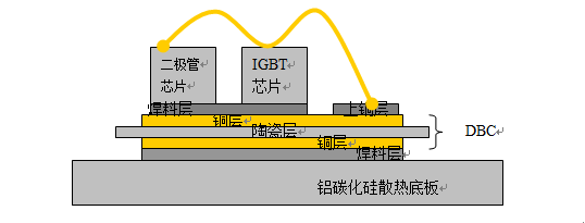
图1 IGBT模块的封装结构
目前,国内外大量研究发现,影响IGBT模块焊接空洞率的因素有[1]:焊接温度、焊接条件、焊料材质、焊料氧化等。本文通过实验发现,底板氧化程度不同对焊接空洞率有较大影响。因此,本文从散热底板氧化的角度来分析其对焊接空洞率的影响,并初步分析了不同氧化程度散热底板与焊接空洞率的关系;此外,本文对改进、优化焊接工艺,提高IGBT模块封装工艺可靠性有重要的实践指导意义。
3二次焊接工艺对IGBT空洞率的影响因素分析
为了分析对比底板氧化程度对焊接空洞率的影响,本实验过程中需要排除二次焊接工艺中其他因素对空洞率所造成的影响。
1、焊料
目前,我们所采用的焊片、焊环材质含有Sn、Pb、Ag,不存在助焊剂,且在焊接之前确保焊料不被氧化。
2、焊接温度
在真空回流焊接过程中,将被焊接的IGBT装载在一个托盘中,并通过电机拖动系统使其依次在加热区、冷却区、真空保压等之间运转。焊接过程中,可根据焊料的熔点温度来选取合适的焊接温度即可,焊接温度完全按照标准的工艺文件设置。
3、还原剂清洗环境
在氮气的保护下进行焊接已经成为IGBT焊接的主流技术,与甲酸技术相结合就能更好的去除清洗工艺。通常,人们使用助焊剂来去除氧化物,可以有效的防止再氧化,但是,助焊剂却会在焊接之后留下残留物,对焊接质量造成不良的影响。因此,我们采用的是在氮气中加入少量且定量的甲酸,即免清洗技术。焊接后不用任何的清洗,且无残留物。
焊接过程中,甲酸的含量在充足与不充足的情况下,对空洞率也是有一定的影响。在操作时,严格按照标准的工艺文件要求,确保好甲酸的含量,以防甲酸对空洞率造成一定的影响。
4、降温速率
在冷却过程中,也需要特别注意降温的速率快慢,特别是在焊料结晶点附近降温速率,降温过快时,便会导致焊料成型的不均匀,当降温速率过慢时,却会导致空洞率的增加,从而影响焊接质量。因此,在实验时,必须按照标准的工艺文件要求来设定速率,以防影响焊接的空洞率。
4 实验过程
为了研究底板氧化程度对焊接空洞率的影响,本文的主要实验过程如图2所示。
SHAPE \* MERGEFORMAT
、
|
一组非氧化底板
|
|
真空焊接炉焊接
|
|
真空焊接炉焊接
|
|
空洞率检测
|
|
空洞率检测
|
|
结果分析 |
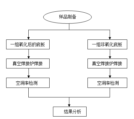
图2 实验流程
4.1 样品制备
选择同一批次的子单元、氧化底板、焊料,将一部分氧化底板进行处理变为非氧化底板。对这两种底板分别进行封装,封装技术按照标准的生产线工艺流程执行,并在同一真空焊接炉里对其进行焊接,确保这两组的焊接条件一致。将这两部分焊接后的模块进行分组,一组是氧化后的底板,一组是非氧化底板。最后,分别选取了4块,在相同实验条件下,对这8块分别进行超声波检测。
4.2 实验条件
空洞的无损检测通常采用超声波检查设备SONOSCAN来检测,通过超声波穿透IGBT模块,其中有缺陷处的空气层可以阻断超声波的传输,即可以分层反应出空洞的尺寸和位置。
对这两组不同的模块进行超声波检查扫描图像,将扫描图载入空洞统计分析软件,计算出每个DBC板焊接区域的焊接空洞占整个焊接表面的百分比率(Window area data)及每个子单元焊接面积的最大空洞面积占该子单元焊接总面积的百分比率(Largest void data)。需要在相同的实验条件下进行多次试验进行对比分析。
4.3 空洞率检测
对选取的4块氧化底板的模块和4块非氧化底板的模块进行相同的实验分析,并计算出各自的焊接空洞率(其中白色亮点即为空洞)。
(1)以一个编号为6430的氧化底板的模块为例,如下图3所示,即超声波检测的扫描图像和空洞所占的面积图:

图3 编号为6430的氧化底板模块空洞率检测图
(2)以一个编号为6613的非氧化底板的模块为例,如下图4所示,即超声波检测的扫描图像和空洞所占的面积图:
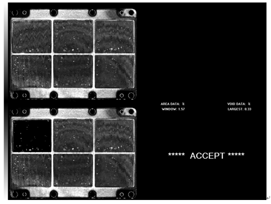
图4 编号为6613的非氧化底板模块空洞率检测图
(3)对两组模块分别进行超声波检测,以每个模块的六个子单元为例,观察空洞率的变化,如下表1所示:
表1 两组模块的空洞率统计表
|
|
氧化底板的模块 |
非氧化底板的模块 |
||||||
|
模块编号 |
6430 |
6435 |
6436 |
6438 |
6613 |
6628 |
6638 |
6642 |
|
Window area data (%) |
5.46 |
3.42 |
4.35 |
6.64 |
1.57 |
1.18 |
1.47 |
0.74 |
|
2.14 |
5.78 |
2.73 |
3.12 |
0.83 |
0.46 |
1.12 |
0.37 |
|
|
2.20 |
3.99 |
6.49 |
3.56 |
1.11 |
0.97 |
1.05 |
0.32 |
|
|
2.21 |
2.93 |
3.64 |
2.57 |
1.40 |
0.38 |
1.49 |
0.30 |
|
|
0.78 |
1.41 |
3.10 |
0.64 |
0.52 |
0.58 |
0.31 |
0.24 |
|
|
2.14 |
2.28 |
4.39 |
1.29 |
0.44 |
0.84 |
0.29 |
0.35 |
|
|
Largest void data (%) |
0.48 |
0.45 |
0.35 |
0.37 |
0.33 |
0.20 |
0.16 |
0.12 |
|
0.17 |
0.64 |
0.23 |
0.28 |
0.13 |
0.08 |
0.09 |
0.09 |
|
|
0.23 |
0.23 |
1.91 |
0.20 |
0.25 |
0.11 |
0.14 |
0.11 |
|
|
0.17 |
0.40 |
0.32 |
0.28 |
0.08 |
0.14 |
0.11 |
0.08 |
|
|
0.11 |
0.10 |
0.28 |
0.04 |
0.10 |
0.16 |
0.07 |
0.04 |
|
|
0.37 |
0.22 |
0.35 |
0.13 |
0.07 |
0.13 |
0.05 |
0.09 |
|
5 结果分析及讨论
5.1 空洞率检测试验结果
通过对这两组模块的超声波检测,根据检测的数据结果分析,氧化底板的模块比非氧化底板的模块焊接空洞率普遍增大,如下表2所示,该表可以直观的看出两组模块焊接空洞率的变化范围。
表2 两组模块的空洞率检测结果对比分析表
|
|
氧化底板的模块 |
非氧化底板的模块 |
|
Window area data (百分比率的变化范围) |
0.78%—6.64% |
0.24%—1.57% |
|
Largest void data (百分比率的变化范围) |
0.04%—0.64% |
0.04%—0.33% |
5.2 结论
通过上述分析,得出以下结论:
1) 散热底板被氧化对IGBT模块焊接的空洞率有明显的影响。如果对氧化后的散热底板进行封装,封装后的IGBT模块焊接空洞率明显提高,达不到超声波检查的质量要求,同时也降低了IGBT模块的性能。
2)超声波检测出氧化底板模块的空洞明显靠近中心位置,相应芯片就越接近高温,失效的可能性也就越大。
6 工艺改进及优化建议
在焊接工艺中,由于IGBT模块封装的工艺中涉及的环节较多,则影响IGBT模块的焊接空洞率的因素就较多,即现有的工艺条件无法避免空洞的形成。那么就需要有效的防止一些可控因素对空洞率的影响。
底板氧化对IGBT模块空洞率的影响可通过一次真空焊接炉高温处理,在真空焊接炉运行过程中,需用无尘纸将每个底板隔开进行高温处理,防止底板的二次污染。经过高温烘干处理后的底板将极大地降低了空洞的存在,从而提高了模块的可靠性和使用寿命。
由于现有的工艺条件有限,应在以后的研究中对防止底板被氧化的工艺进行改进,以期进一步降低空洞率
7 参考文献
[1] 徐玲,周洋,张泽峰,陈明祥,刘胜. IGBT模块焊料层空洞对模块温度影响的研究.中国电子科学研究院学报[J],2014(2):125~129
[2] 张泉.高压IGBT模块基板焊接工艺研究.大功率变流技术[J],2011(3):5~7
[3] 周洋,徐玲.IGBT模块回流焊工艺中预翘曲铜基板的研究.中国电子科学研究院学报[J],2013(12):578~582
[4] 唐勇,汪波,陈明,刘宾礼.高温下的IGBT可靠性与在线评估.电工技术学报[J],2014(6):17~23
在线预约 >
BaTiO3复合硅胶对 IGBT 模块内部电场分布的影响 王昭,刘曜宁 (中车永济电机有限公司 半导体分公司,陕西 西安 710018) 摘要: 随着 IGBT 高压功率模块的发展,模块内部电场绝缘问题也显得越来越重要。功率模块封装中使用的硅 凝胶的电场承受能力直接影响了整个模块的绝缘表现。目前已经有学者研究了一系列方法来优化电场表现,提高可 靠性。本文通过使用有限元分析方法,分析和确定模块中最大电场存在的位置并提出相应的优化解决方案。 关键词: IGBT 模块;硅胶;BaTiO3;有限元分析;电场模拟;局部放电 中图分类号: TM215.92 文献标识码:A 文章编号:
在线预约 >SiC电力电子器件在牵引领域应用展望*
曹琳+,郑松,吴磊,冯科
(中车永济新时速电机电器有限责任公司,山西 永济 044502;
西安永电电气有限责任公司,陕西 西安 710016)
摘要:宽禁带半导体SiC是最有发展前途的电力电子材料,满足牵引变流器轻量化、小型化、高效化的发展趋势。本文阐述了SiC电力电子器件在牵引领域的应用现状,介绍了SiC SBD、SiC MOSFET、SiC JFET及SiC IGBT的优势及特点,论证了SiC电力电子器件在牵引领域应用面对的挑战。可以看到的是,随着SiC单晶质量及晶片尺寸,相关制造、封装工艺的成熟与完善,用不了多少年,牵引领域电力电子装置和系统的性能就会因为SiC器件的广泛应用而得到显著的提升。
关键词:SiC,电力电子器件,牵引
Development and Prospect of SiC Power Devices
in Electric Traction
CAO Lin, ZHENG Song, WU Lei, FENG Ke
(CRRC YongJi Xinshisu Electric Equipment Co., Ltd., YongJi 044502, CHN
Xi’an Yong Dian Electric Co., Ltd.,Xi’an710016, CHN;)
Abstract: The wide band gap semiconductor Silicon Carbide (SiC) is the most promising power electronic materials that in accordance with electric traction converters lightweight, compact and high efficient development trend. This paper describes the current application status of SiC power devices in electric traction field, introduces the SiC SBD, SiC MOSFET, SiC JFET and SiC IGBT advantages and characteristics, demonstrates the challenges of SiC power devices in the electric traction driven system. In the foreseeable future, with the development and mature of SiC single crystal quality, wafer size, related manufacturing and encapsulation technology, it does not take many years, the power electronic traction equipment and system performance will be significantly improved because of SiC devices widely use.
Keywords: SiC, power electronics, traction
1 引言
电牵引技术的不断发展要求电力电子器件具有更高的功率密度、更高的工作温度、更小的功率损耗、更快的开关速度[1]。以硅(Silicon-Si)材料为基础的电力电子器件因大功率场效应晶体管(功率MOSFET)和绝缘栅双极晶体管(IGBT)等新型电力电子器件的应用而日趋成熟。随着器件结构设计及制造工艺的完善,当前器件的性能已经接近Si材料的理论极限[2]。目前,以碳化硅(SiC)为代表的第三代宽禁带半导体电力电子器件已经实现商品化,在牵引领域表现出巨大的潜力[3]。
SiC材料较大的禁带宽度(3.26eV)使其相比于Si材料(1.12eV)具有很大的优势:本征载流子浓度低20个数量级,临界击穿电场高10倍,热导率高3倍,电子饱和漂移速率高1倍等。这些特性使得SiC电力电子器件在高温、高频及阻断电压等方面突破Si材料的极限[4]。
目前,SiC电力电子器件已经在600V-1700V中低压领域实现了产业化,Cree、Rohm、Infineon等公司可批量供应最大电流50A的SiC SBD及MOSFET产品,其应用已显著提高系统工作频率及整机效率。高压SiC器件[5]早在2003年已有报道,然而受晶体质量[6]及相关工艺限制,其产业正在发展中。机车牵引、高压直流输变电等领域目前正小批量试用高压SiC器件,系统性能提升明显。
牵引领域,2007年开始,丰田、日产[7]、本田等公司首先将SiC器件应用于电动汽车(EV)中。同时,罗姆、三菱、东芝等半导体公司也针对电动汽车需求开发SiC产品,以满足牵引逆变器小型化、轻量化、高效率的发展趋势。机车牵引领域,日本三菱电机于2011年10月推出SiC功率逆变器用于东京地铁银座线“01系”的部分车辆,用以进行车辆运行考核。2014年推出1500A/3300V 全SiC模块[8]用于小田急1000系列列车。日立公司也于2012年4月发布了针对地铁车辆用于1.5kV直流接触网的3.3kV 混合SiC模块。SiC电力电子器件在牵引领域应用正由样机试验试制阶段向批量化生产和工程化应用靠近。
我国高铁建设目前已拥有世界领先水平,但牵引用SiC电力电子器件及应用尚处于初期阶段。2013年开始,中国中车永济电机[9]及株洲时代电气[10]开始进行SiC器件封装及应用研究,希望通过应用推动整个SiC电力电子产业链的发展,追赶国外先进技术的脚步。
2 SiC电力电子器件
SiC器件在高阻断电压下依然有很小的导通电阻,因此SiC器件的研究开始集中在肖特基势垒二极管(SBD)、MOSFET等少数载流子器件上。
2.1 SiC SBD
SiC SBD为单极性器件,没有少数载流子的注入及自由电荷的存储,具有几乎理想的反向恢复特性,适合在高压、高频及高温条件下工作。
由于高压下SiC肖特基势垒比Si薄[11],进一步提高SiC SBD的反向电压会受到隧穿势垒引起的反向漏电流限制。为了充分发挥SiC临界击穿电场高的优势,通常采用JBS[12]、MPS等结构降低肖特基接触处电场强度,获得了较好的器件特性。
SiC SBD是发展最为成熟的SiC电力电子器件,适用于600V-3300V阻断电压范围。Cree、Rohm、Microsemi、Infineon等公司SiC SBD已经应用于变频或者逆变装置中替换Si基快恢复二极管,显著提高了工作频率和整机效率。然而由于SiC开关器件发展的相对滞后,因此目前在牵引、工业变频等领域的普遍做法是将SiC SBD和Si IGBT芯片封装在一起以形成大功率开关器件,以降低器件开关损耗。
2.2 SiC MOSFET
SiC是唯一具有热氧化层的宽禁带半导体材料,因此可以直接借鉴Si 基MOSFET的设计、制造经验和生产设备。同时,SiC MOSFET与现有Si基MOSFET、IGBT驱动电路兼容,因此SiC MOSFET是发展最快的开关器件。
SiC MOSFET早期发展存在一些问题,如沟道迁移率低和栅氧化层可靠性问题。目前,迁移率问题通过埋沟[13]、高温气氛氧化等设计、工艺技术得到基本解决。可靠性方面,350°C[14]下栅氧化层依旧具有良好的可靠性,目前已经不是限制SiC MOSFET发展的瓶颈。
2012年,日本Rohm公司通过优化工艺条件及器件结构,改善了晶体质量,首次实现了SiC SBD与SiC MOSFET一体化封装,解决了1200V级别逆变器中使用Si IGBT及FRD(快恢复二极管)而导致功率转换损耗较大的问题。该产品在降低器件工作损耗70%以上的同时还实现了100kHz以上更高的工作频率,推动了外围部件小型化的发展。预计在今后5-10年时间,SiC MOSFET将替代Si IGBT成为主流电力电子开关器件。
2.3 SiC JFET
由于SiC MOSFET结构存在的不完美特性,使得同样为单级性开关器件的SiC JFET(结型场效应晶体管)受到了重视,并与SBD、MOSFET率先实现了商业化。SiC JFET还具有阈值电压随温度稳定性好、高温可靠性高等优点,是目前发展较快的SiC开关器件。
然而栅极P-N结工作方式的特点对器件应用也带来了很多不利的影响,如常通型、高米勒电容(Miller Capacitor)效应、高负栅关断电压等问题。这使得SiC JFET不能直接替代Si MOSFET及IGBT,使用时需要对驱动电路作出相应的调整,以保证器件安全可靠的工作。
目前,SiC JFET器件已经实现一定程度的产业化,主要以Infineon、SiCED及Semisouth公司的产品为主。产品电压等级在600V、1200V、1700V,单管电流最高达20A,模块电流等级达到100A以上。2013年,Rockwell 公司采用600V/5ASiC增强型JFET以及SiC SBD并联制作了25A三相电机驱动模块,与当时先进的Si IGBT模块相比较,同等功率下芯片面积减少40%,同时损耗及开关过电压、过电流问题降低明显。
2.4 SiC IGBT
受P型衬底电阻率高、沟道迁移率低及栅氧化层可靠性问题限制,SiC IGBT的研发工作起步较晚,1999年才有报道。经过多年的研究,目前已经逐步解决了上述问题。2008年报道的13kV[15] N沟道SiC IGBT通态比电阻达到了22mΩ.cm2。
通过与SiC MOSFET、Si IGBT及晶闸管比较发现,在阻断电压15kV以上领域,SiC IGBT综合了开关速度快及功耗低的特点,具有明显的优势。因此,通过不断提升SiC IGBT芯片特性及可靠性,SiC IGBT将成为智能电网中的核心器件。
3 SiC电力电子器件在牵引领域应用面对的挑战
3.1 芯片制造成本过高
从商业化角度看,SiC功率器件在电力电子器件市场很大,但SiC能否成功打入牵引领域市场,最终还是取决于它的性价比。目前虽已实现了6英寸4H-SiC衬底制备,但Cree公司从2英寸(1997年)扩大到商业化6英寸(2010年)零微管4H-SiC衬底花费了13年时间。同时,SiC功率器件工艺费用也很高,设备及技术掌握在国外少数几家公司。较高的价格导致其通常应用在高温,辐照等Si器件不能应用的领域。较小的市场维持高的成本限制了SiC功率器件的发展。
目前,同一规格SiC功率器件的价格是Si器件的5-6倍,当这一数值降到2-3倍时,SiC功率器件将会大范围应用于电动汽车、机车、动车变流器中,推动牵引系统快速发展。
3.2 材料缺陷多,单个芯片电流小
虽然目前SiC器件的研究已经取得了非常瞩目的成果,但其性能离SiC材料本身的极限还有较大距离。近几年,利用物理气相传输法(PVT)生长的SiC晶体和化学气相沉积法(CVD)生长的SiC薄膜取得了惊人的进步。采用缓冲层、台阶控制外延及位置竞争等技术制备的SiC薄膜晶体质量有了很大的提高,并实现了可控掺杂。但晶体中仍含有大量的微管[16]、位错[17]和层错[18]等缺陷,这些缺陷严重限制了SiC芯片成品率及大电流需求。
SiC电力电子器件要想应用于牵引领域,单个芯片面积必须要在1.2cm2以上,以保证100A以上的通流能力,降低多芯片并联产生的寄生参数。因此,SiC材料必须解决上述缺陷问题,SiC器件才有可能在牵引领域批量应用。
3.3 器件封装材料与技术有待提高
目前SiC功率器件封装工艺及方法通常借鉴Si IGBT封装技术,在DBC布局、芯片键合、高温焊料、硅凝胶填充、密封材料等方面还存在一些问题,不能充分发挥SiC材料高温及高频应用的优势。
针对SiC器件封装特殊要求,三菱、塞米控、富士等公司在封装材料及结构方面提出了新的思路,如三菱公司铜针布线技术,塞米控公司低温纳米银烧结技术,富士公司低电感和优化的DBC布局设计。随着国际厂商对SiC封装技术的重视,封装材料的不断发展及封装结构优化,封装将不再是限制SiC器件性能的瓶颈,SiC材料优势将完全得到展现。
4 结论
相比于目前广泛应用的Si电力电子器件,SiC器件可工作于更高的开关频率,实现电容及电感等储能和滤波部件小型化;芯片功率密度更大,缩小器件及功率模块尺寸;损耗小,工作结温高,减小冷却装置体积。这些优良特性共同推动牵引变流器向小型化、轻量化、高效率的方向发展。目前,由SiC SBD与SiC MOSFET组成的开关器件已经开始应用于机车牵引领域,展现出了优越的性能。
当前制约SiC电力电子器件在牵引领域应用的主要因素包括:衬底及外延成本高,芯片价格高;材料缺陷多,芯片成品率及单只芯片电流受到限制;封装技术存在瓶颈,SiC材料性能无法得到完全展现。不过可以看见的是,随着SiC材料技术的不断发展及各大厂商对SiC器件的重视,SiC电力电子器件未来几年在成品率、可靠性、价格及封装技术方面可获得较大改善,将广泛应用于牵引领域,逐步展现出其性能和降低变流系统成本方面的优势,对牵引变流器的发展和变革产生持续的推动作用。
参考文献
1 丁荣军. 现代轨道牵引传动及控制技术研究与发展[J]. 机车电转动,2010(5):1-8.
2 陈治明,李守智. 宽禁带半导体电力电子器件及其应用[M]. 北京:机械工业出版社,2009.
3 郝跃,彭军,杨银堂. 碳化硅宽带隙半导体技术[M]. 北京:科学出版社,2000.
4 陈治明,王建农. 半导体器件的材料物理学基础[M]. 北京:科学出版社,2004.
5 J. H. Zhao, p. alexandrov, X. Li. Demonstration of the first 10-kV 4H-SiC Schottky barrier diodes [J], IEEE Electron Device Letters, 2003, 24(6): 402-404.
6 R. Singh, J. A. Cooper, M. R. Melloch, J.W Palmour, T. P. Chow. SiC power Schottky and PiN diodes [J], IEEE Transactions on Electron Devices, 2002, 49(4): 665-672.
7 Cooke M. Wide load potential for electric vehicles [J], compounds &advance silicon, 2009, 4(5):70-75.
8 Kenji Hamada, Shiro Hino, Naruhisa Miura[J], Japanese Journal of Applied Physics, 2015, 54(07):1-4.
9 曹琳, 王富珍.100A/1200V Si/SiC混合模块对比研究[J]. 固体电子学研究与进展,2015, 3(3):221-226.
10 邵云, 史晶晶, 李城瞻, 彭勇殿. 高性能碳化硅混合功率模块研制[J]. 大功率变流技术,2013, 2(1):57.
11 A. Itoh, T. Kimoto, H. Matsunami. High performance of high voltage 4H-SiC Schottky barrier diodes [J], IEEE Electron Device Letters, 1995, 16(6): 280-282.
12 Raghunathan R, Alok D, Baliga B J. High voltage 4H-SiC Schottky barrier diodes [J], IEEE Electron Device Letters, 1995, 16(6): 226-227.
13 李宇柱. SiC电力电子技术综述[J]. 固体电子学研究与进展,2011, 31(3):213-217.
14 盛况,郭清,张军明,钱照明. 碳化硅电力电子器件在电力系统的应用展望[J]. 中国电机工程学报,2012, 32(30):1-6.
15 Akira S, Hajime O, Tsunenobu K. A 13kV 4H-SiC n-Channel IGBT with low Rdiff,on and fast switching[J]. Material Science Froum, 2009, 600(1):1183-1186.
16 P. G. Neudeck, J.A. Powell. Performance limiting micropipe defects in silicon carbide wafers [J], IEEE Electron Device Letters, 1994, 15(2): 63-65.
17 Q. Wahab, A. Ellison, A. Henry, E. Janzén, C. Hallin, J. Di Persio, R. Martinez. Influence of epitaxial growth and substrate-induced defects on the breakdown of 4H-SiC Schottky diodes [J], Applied Physics Letters, 2000, 76(19): 25-27.
18 Zhang X, Ha S, Benamara M. Structure of Carrot Defects in 4H-SiC Epilayers [J], Materials Science Forum, 2006, 527-529: 327-332.
作者简介:
姓名:曹琳;工作单位:中车永济新时速电机电器有限责任公司;职务:无;专业技术职务:电气工程师;研究领域:SiC芯片及模块应用研究、Si基IGBT芯片后道工艺、IGBT模块结构设计、可靠性及失效分析研究;通信地址:陕西省西安市经开区凤城十二路中国中车永济电机研发中心;联系电话:13572966628;电子邮箱:cl_zhifang@hotmail.com;邮编:710016。
在线预约 >
The HiPak power semiconductor module series is designed for reliable operation under demanding conditions throughout the module’s lifetime. The operation conditions and thus the expected module’s lifetime strongly depends on the application. In operation, the modules are subjected to a variety of temperature profiles, which cause cyclic thermo-mechanical stress in all components and joints of the modules and finally lead to device failure. The magnitude and frequency of these stress-cycles define the lifetime expectancy. Each specific profile leads to different stress distribution throughout the module, so that the weakest link of the module, which finally leads to failure, can be found in different components or joints. Moreover it is not possible to calculate the exact lifetime of individual modules. Instead the lifetime must be expressed in terms of the B10 lifetime, which is the number of cycles during which 10 percent of the total number of modules fails. The aim of this application note is to provide load cycling lifetime data for the power electronics designer to estimate the module lifetime for optimisation of the particular application.
在线预约 >
Comparison study of100A/1200V Si/SiC Hybrid IGBT Modules
Cao Lin (曹琳), Wang Fu-Zhen (王富珍),
Xi’an Yong Dian electric Co., Ltd
Abstract-In this paper a comparative study of SiC SBD in IGBT module is presented. The static and dynamic character were measured and analyzed. It is shown that the IGBT switching losses can be drastically reduced by replacing the silicon freewheeling PiN diode with SiC SBD. That enables the hybrid module more efficiency and capable of shrink the size of the power system by increasing the switching frequency. In order to explain the current and voltage oscillation during turn-on process of the hybrid module, this paper looks into the different current paths during turn-on and turn-off of the IGBT module to illustrate the conditions for oscillation. The oscillation is LC resonant that triggered by not only the stray inductance of the package but also the device capacitance in the IGBT and the freewheeling diode. Therefore, further work is necessary in low parasitic inductance package technology for SiC device, the system performance and reliability can be improved.
Keywords: IGBT module; SiC SBD; switching losses; oscillation
PACC: 2520M; 2560P; 2560H
The insulated gate bipolar transistor (IGBT) combines both the merit of MOS and bipolar structures to achieve a voltage driven power device with low on-state voltage, low switching losses and high current density, which has become the best choice for a wide range of industrial power conversion applications.
For satisfy the ever-increasing demand in power electronics applications, the designers have expended significant effort to improve system efficiency, decrease size and weight, reduce cooling equipment. All of these requirements are greatly influenced by the power dissipation that includes conduction, turn-on and turn-off losses. Lots of efforts have been done to reduce conduction and turn-off losses, such as trench field[1] stop technology and lifetime control in the buffer layer to optimize device characteristics. However, the IGBT turn-on losses are restricted depend on the freewheeling diode reverse recovery current. Thus, freewheeling diode with zero recovery charge is desirable during turn-on process.
It is shown that the superior properties enable wide bandgap silicon carbide (SiC) power devices capable of operating at higher frequencies, higher voltages, and higher temperatures. The SiC Schottky barrier diode (SBD) is now commercially available with breakdown voltage ratings of 600V-1700V and1A-60Acurrent ratings. The reverse-recovery charge in SiC SBD is extremely low and is the result of junction capacitance, not stored charge. Furthermore, unlike Si PiN ultra fast diodes, the reverse recovery character is independent on di/dt, forward current and temperature. Thus, SiC SBD as freewheeling diode in IGBT module may improving the system efficiency, lower the case temperature and reduced cooling equipment, conform IGBT module development trend.
In order to investigate the benefit of SiC SBD in IGBT module, both static and dynamic characters were measured and analyzed by comparison method in this paper. Meanwhile, the different current paths during turn-on and turn-off were analyzed in order to explain the current and voltage oscillation during hybrid module turn-on process.
In order to illustrate the benefit of SiC hybrid module, we have developed two types half-bridge module with 1200V,100Apower rating by commercially released chip. The hybrid module consists of four Si IGBT (50Aper IGBT) with eight anti-parallel SiC SBDs (20Aper diode). Another Si module consists of four Si IGBT (50Aper IGBT) with four anti-parallel Si PiN freewheeling diodes (50Aper diode). The Si IGBTs, Si PiN diodes, and the SiC SBDs are attached on the direct bond copper (DBC) substrate with minimum inductance loop. The solder joints both die and substrate, substrate and baseplate by the reflow solder systems. The top-side die contact is done with 15 mil Aluminum wires. Finally, the module is put in a plastic case filled with silicone gel for protection and insulation.
The main static characteristic of the two type module is show in table 1.
Table. 1 main static characteristic of the two type module
|
|
VGEth @25°C |
VCEsat @25°C |
VF @25°C |
VF @125°C |
ICES @25°C |
ICES @125°C |
|
Si |
5.95 V |
1.811 V |
1.797 V |
1.817 V |
0.0026 mA |
1.13 mA |
|
Hybrid |
5.94 V |
1.805 V |
1.565 V |
1.965 V |
0.0414 mA |
0.322 mA |
The gate-emitter threshold voltage (VGEth) and collector-emitter saturation voltage (VCEsat) are mainly decided by the Si IGBT chips, is nearly the same of both two type modules. Due to much low barriers, the anode-cathode on-state voltage (VF) of the SiC SBD is lower than Si PiN diode at room temperature. Meanwhile, SiC SBD exhibited strong positive temperature coefficient, is unlikely to create a current imbalance, even when multi-parallel connection. The leakage current (ICES) of the hybrid module is about 16 times larger than that of the Si module at room temperature due to low Schottky barriers. However, due to wide bandgap, there are few thermal excited carriers at high temperature, thus the leakage current of SiC SBD is less affected by temperature. The increased leakage current of hybrid module at 125 ° C is dominated by Si IGBT chips, is much less than Si module, that character enable SiC SBD operation at junction temperatures of up to 175 ° C.
The switching characters of the module were measured using a double pulse tester (DPT) with 2000μH inductive load. The self-heating of the devices is neglected due to the slow thermal time constant compared to the double pulse duration.
Compared with Si PiN diode, the main advantage of SiC SBD is its superior dynamic performance. The reverse-recovery charge in the SiC SBD is extremely low[5] and is the result of junction capacitance, not stored charge, thus best suited for fast switching application.
Figure 1 shows the measured turn-on waveform of the hybrid and Si module. The hybrid module results in a peak current (ICpk) of136A, which can be reduced significantly by 43.6% compared to the Si module.
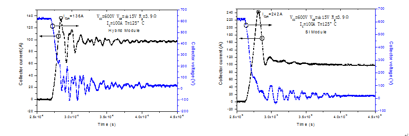
Figure 1. Turn-on waveforms of the two type IGBT module.
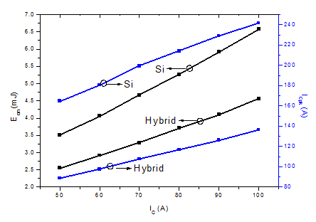
Figure 2. IGBT turn-on loss and peak current according to collector current.
The influence of the collector current on the IGBT turn-on loss and peak current can be found in figure 2. The turn-on loss is dominated by the overshoot current due to the reverse recovery charges of the freewheel diode, thus the hybrid module reduced 30.7% turn-on losses compared with Si module. The reduction in turn-on losses will improve the components efficiency and shrink the size of high power system by increasing the switching frequency.
Figure 3 shows the turn-off waveforms of the hybrid and Si module. The turn-off surge voltage (VCEpk) of the hybrid module is 25V lower than that of the Si module at100Acurrent rate. The turn-off losses of hybrid module are 7.4% lower than the Si module as figure 4 shown. In this case, the package configuration of the two type module is same, therefore the main circuit inductance are equal. The difference in the surge voltages may originate from the difference of the transient on-state voltages between SiC SBD and Si PiN diode.
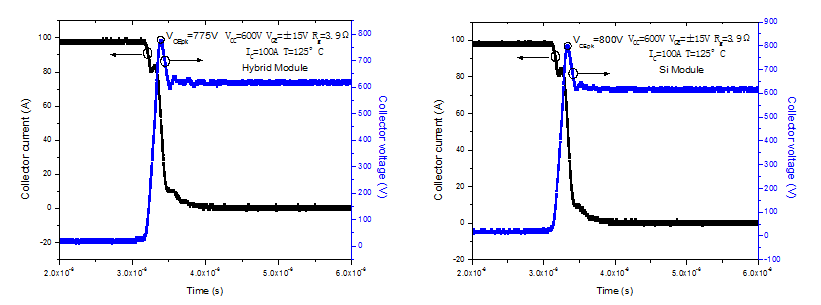
Figure 3. Turn-off waveforms of the two type IGBT module.
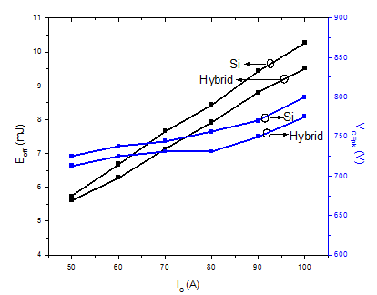
Figure 4. IGBT turn-off loss and peak current according to collector current.
The voltage and current oscillation occurred during turn-on process of the hybrid module as figure 1 shown. The IGBT switching oscillations has been discussed in some paper[8][9], and may have two possible sources. In this particular case, oscillations may come from the resonant circuit caused by the stray inductance in the package and the capacitance of the device. This section discussed the different current paths during turn-on and turn-off processes of the IGBT module for the sake of explain this particular phenomenon.
The current path during turn-on process is shown in figure 5.
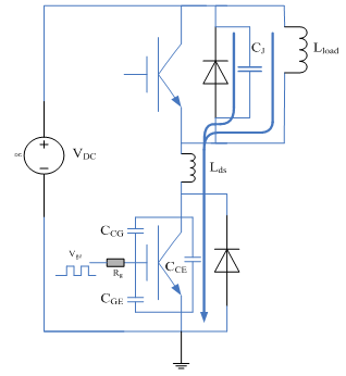
Figure 5. Current paths during turn-on process.
The turn-on oscillation occurs after the IGBT current reaches the load current as figure 1 shown. After this period, the current in the freewheeling diode is transferred to the IGBT, so the diode current decrease from its forward current (equal to load current IL) at an identical rate. After the IGBT has taken all the load current, the collector-emitter voltage (VCE) starts to fall and the freewheeling diode stops conducting, the charge store in the diode has been removed and its voltage reversed. Thus the diode junction capacitance CJ gets charged and the IGBT output capacitance COES gets discharged as figure 5 shown. Therefore the voltage and current oscillation during turn-on process should be LC-oscillation caused by the tray inductance Lds resonating with diode junction capacitance CJ and the IGBT output capacitance COES.
In the Si module of this work, the junction capacitance CJ of the PiN diode is much smaller than the IGBT output capacitance COES that is given in the datasheet. Therefore CJ in series with COES result in a capacitance close to CJ. However, in the hybrid module, due to the one decade higher critical field strength, SiC device allows two decades higher drift layer doping at the same breakdown voltage, the CJ of SiC SBD is one decade higher than Si PiN diode. Therefore, the capacitance in the hybrid module turn-on resonant circuit is much larger than Si module. This can be explaining why hybrid module exhibit more obvious oscillation than Si module.
Such an oscillation is unacceptable in the IGBT module because it’s greatly reduced reliability, possibly reduced efficiency and produced radio frequency noise. Increasing gate resistance is often effective in reducing the oscillations in the first place, but higher gate resistance also leads to increased IGBT turn-on losses, the advantages of the hybrid module were lost. Recently, Lots of work has been down to eliminates oscillation while minimizing switching losses, such as reduces the parasitic inductance in the commutation loop to suppresser the LC-resonance or ferrite bead methods. Therefore, the change from Si to SiC technology is not an easy path and lots of work must be carefully considered in the designing process of the SiC module.


